Overview:
New research: Gravitational metamaterials
We are currently involved in research on metamaterials. This new field has been popularized in the media through numerous reports of emerging metamaterials applications such as negative refraction, flat lenses, and optical, thermal and microwave “cloaking” devices. In essence, metamaterials offer the potential to make objects invisible to heat, light, and microwaves. However, a fundamental limitation of most metamaterials is that they tend to be inherently narrowband, working over a small range of frequencies. Thus, a focus of our research is the development of new methods to overcome such bandwidth limitations. In particular, we are investigating the use of non-Foster integrated circuits, such as negative capacitors and negative inductors, to create wideband metamaterials.
Further Details:
Team Members and Contributors:
Drs. Weldon, Adams, and Daneshvar serve as the principal investigators on the project. Graduate students who have contributed to the project include J. Shehan, J. Covington, V. Kshatri, K. Smith, and K. Miehle. Undergraduate students who have contributed through their senior design projects include C. Boneque-Santos and A. Tarabichi.
-
- Konrad Miehle, Thomas P. Weldon, Ryan S. Adams, and Kasra Daneshvar, “Wideband Negative Permeability Metamaterial with Non-Foster Compensation of Parasitic Capacitance,” to appear in 2012 IEEE International Symposium on Antennas and Propagation and USNC-URSI National Radio Science Meeting, Chicago, IL, July 8-14, 2012.
- Thomas P. Weldon, Konrad Miehle, Ryan S. Adams, and Kasra Daneshvar, “A Wideband Microwave Double-Negative Metamaterial with Non-Foster Loading,’ “A Wideband Microwave Double-Negative Metamaterial with Non-Foster Loading,” IEEE SoutheastCon 2012 Proceedings, pp. 1-4, Orlando, FL, March 15-18, 2012.
- Thomas P. Weldon, Konrad Miehle, Ryan S. Adams, and Kasra Daneshvar, “Simulation, Measurement, and Parameter Extraction for a 5.8 GHz Negative Permittivity Metamaterial,” IEEE SoutheastCon 2012 Proceedings, pp. 1-4, Orlando, FL, March 15-18, 2012.
- Joshua W. Shehan, John M. C. Covington III, Varun S. Kshatri, Thomas P. Weldon, Ryan S. Adams, “Permeability and Permittivity Extraction Issues For Non-Foster and Active Metamaterials,” 2013 IEEE International Symposium on Antennas and Propagation and USNC-URSI National Radio Science Meeting , Orlando, FL, July 7-13, 2013.
- Joshua W. Shehan, Ryan S. Adams, Thomas P. Weldon, “A Coaxial Test Fixture for Transmission/Reflection Measurements of Metamaterials,” 2013 IEEE International Symposium on Antennas and Propagation and USNC-URSI National Radio Science Meeting , Orlando, FL, July 7-13, 2013.
- Varun S. Kshatri, John M. C. Covington III, Joshua W. Shehan, Thomas P. Weldon, Ryan S. Adams, “Comparison of CMOS Current Conveyor Circuits for Non-Foster Applications,” IEEE SoutheastCon 2013 Proceedings , pp. 1-4, Jacksonville, FL, April 4-7, 2013.
- Varun S. Kshatri, John M. C. Covington III, Joshua W. Shehan, Thomas P. Weldon, Ryan S. Adams, “A DC-Coupled Negative Inductance Circuit with Integrated Bias,” IEEE SoutheastCon 2013 Proceedings , pp. 1-4, Jacksonville, FL, April 4-7, 2013.
- Varun S. Kshatri, John M. C. Covington III, Joshua W. Shehan, Thomas P. Weldon, Ryan S. Adams, “Capacitance and Bandwidth Tradeoffs in a Cross-Coupled CMOS Negative Capacitor,” IEEE SoutheastCon 2013 Proceedings , pp. 1-4, Jacksonville, FL, April 4-7, 2013.
- Thomas P. Weldon, Ryan S. Adams,and Joshua W. Shehan, “Stability of Embedded Non-Foster Metamaterials with Potentially Unstable Circuit Parameters,” Seventh International Congress on Advanced Electromagnetic Materials in Microwaves and Optics – Metamaterials 2013 , Bordeaux, France, Sept. 16-19, 2013.
- Varun S. Kshatri, John M. C. Covington III, Kathryn L. Smith, Joshua W. Shehan, Thomas P. Weldon, and Ryan S. Adams “Measurement and Simulation of a CMOS Current Conveyor Negative Capacitor for Metamaterials,” IEEE SoutheastCon 2014 Proceedings , pp. 1-4, Lexington, KY, Mar. 13-16, 2014.
- John M. C. Covington III, Kathryn L. Smith, Joshua W. Shehan, Varun S. Kshatri, Thomas P. Weldon, and Ryan S. Adams “Measurement of a CMOS Negative Inductor for Wideband Non-Foster Metamaterials,” IEEE SoutheastCon 2014 Proceedings , pp. 1-4, Lexington, KY, Mar. 13-16, 2014.
- John M. C. Covington III, Kathryn L. Smith, Varun S. Kshatri, Joshua W. Shehan, Thomas P. Weldon, and Ryan S. Adams “A Cross-Coupled CMOS Negative Capacitor for Wideband Metamaterial Applications,” IEEE SoutheastCon 2014 Proceedings , pp. 1-4, Lexington, KY, Mar. 13-16, 2014.
- Varun S. Kshatri, John M. C. Covington III, Thomas P. Weldon, and Ryan S. Adams “Compensation of Frequency Dependent Parasitic Resistance in a CMOS Linvill Negative Inductor,” IEEE SoutheastCon 2014 Proceedings , pp. 1-4, Lexington, KY, Mar. 13-16, 2014.
- John M. C. Covington III, Varun S. Kshatri, Thomas P. Weldon, and Ryan S. Adams “Parasitic Resistance in Non-Foster Circuits Caused by Current Conveyor Frequency Response,” IEEE SoutheastCon 2014 Proceedings , pp. 1-4, Lexington, KY, Mar. 13-16, 2014.
- Kathryn L. Smith, Ryan S. Adams, and Thomas P. Weldon, “A Novel Broadband Fractal Metamaterial Unit Cell,” in 2014 IEEE International Symposium on Antennas and Propagation and USNC-URSI National Radio Science Meeting , Memphis, TN, July 6–12, 2014.
- Thomas P. Weldon, John M. C. Covington III, Kathryn L. Smith, and Ryan S. Adams “Performance of Digital Discrete-Time Implementations of Non-Foster Circuit Elements,” 2015 IEEE International Symposium on Circuits and Systems (ISCAS 2015), Lisbon, Portugal, May 24-27, 2015.
- Kathryn L. Smith, Thomas P. Weldon, and Ryan S. Adams, “Measurement, Simulation, and Theory of a Non-Foster Metamaterial Unit Cell with Parasitic Resistance,” 2015 IEEE International Symposium on Antennas and Propagation and USNC-URSI National Radio Science Meeting, Vancouver, BC, Canada, July 19-25, 2015.
- Thomas P. Weldon, John M. C. Covington III, Kathryn L. Smith, and Ryan S. Adams, “Stability Conditions for a Digital Discrete-Time Non-Foster Circuit Element,” 2015 IEEE International Symposium on Antennas and Propagation and USNC-URSI National Radio Science Meeting, Vancouver, BC, Canada, July 19-25, 2015.
- Thomas P. Weldon and Ryan S. Adams, “Digital Discrete-Time Non-Foster Approach to Broadband Fast-Wave Microstrip Lines,” Ninth International Congress on Advanced Electromagnetic Materials in Microwaves and Optics – Metamaterials 2015, Oxford, United Kingdom, Sep. 7-10, 2015.
- Thomas P. Weldon, John M. C. Covington III, Kathryn L. Smith, and Ryan S. Adams, “A Two-Port Digital Discrete-Time Non-Foster Circuit Designed for Negative Capacitance,” Ninth International Congress on Advanced Electromagnetic Materials in Microwaves and Optics – Metamaterials 2015, Oxford, United Kingdom, Sep. 7-10, 2015.
-
K. Smith, “The use of fractals and non-Foster circuits for wideband metamaterials and antennas,” Master’s thesis, University of North Carolina at Charlotte, 2015. (filePassWrd=smith)
- Thomas P. Weldon, Ryan S. Adams, Konrad Miehle, US patent pending 13/766,249, “Wideband Negative-Permittivity Metamaterials and Negative-Permeability Metamaterials Utilizing Non-Foster Elements,” Feb. 13, 2013.
- T. P. Weldon, “Digital discrete-time non-Foster circuits and elements,” International Patent Application No. PCT/US2015/27789, Apr. 27, 2015, published on WIPO as WO2015164866, Oct. 29, 2015..
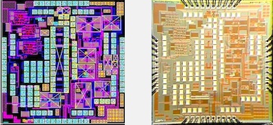
Recent Non-Foster Integrated circuits:
Non-Foster integrated circuits are being designed in 0.5 micron CMOS to create negative capacitors and negative inductors. Below, the image on the left is the layout using Cadence design tools, the image on the right is a photograph of the fabricated integrated circuit chip with wire bonds attached to 40 of the ~150 available bonding pads.
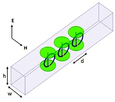
Recent Wideband Microwave Metamaterials:
Recent HFSS simulations of the microwave metamaterial structure below show potential for over two octaves of double-negative metamaterial performance using non-Foster loading of the electric and magnetic structures.
Note: This material is based upon work supported by the National Science Foundation under Grant No. 1101939. Any opinions, findings, and conclusions or recommendations expressed in this material are those of the author(s) and do not necessarily reflect the views of the National Science Foundation.


